| Samsung Display has decided to use CVD (Chemical Vapor Deposition) system from Applied Materials, an American semiconductor system manufacturer that is at the top of the market, temporarily after it initially decided to use WONIK IPS’ CVD system for QD (Quantum Dot) display that is currently going through a mass-production phase as Samsung Display’s next-generation technology. Although WONIK IPS has looked for an opportunity to expand its business towards the CVD market after years of R&D, it lost its first opportunity to Applied Materials.
According to the industry, Samsung Display has temporarily decided to replace WONIK IPS with Applied Materials as the supplier of CVD system, which is one of major front-end processes, before it places an order for necessary facilities and equipment for QD display. Main executives of Samsung Display recently visited Applied Materials’ headquarters and discussed about Applied Material’s CVD systems.
Initially, Samsung Display had been working with WONIK IPS to separate the supply network of CVD systems. TFE (Thin Film Encapsulation) process that forms thin organic films and inorganic films one after the other in order to protect organic matters from water and oxygen is the process that Samsung Display has been preparing to separate the supply network. Applied Materials’ CVD system forms inorganic films.
Samsung Display is currently only using Applied Materials’ CVD systems for its 6th Gen OLED production lines.
However, it was looking for a change for 8th Gen QD display. WONIK IPS, which is one of Samsung Display’s key partners, had participated in R&D process of QD Display and focused on developing a system that can replace Applied Materials’ systems.
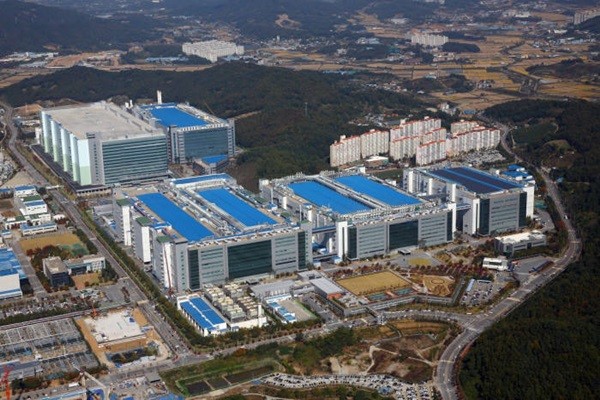
 <Samsung Display’s Asan Campus (Source: Samsung Display)> <Samsung Display’s Asan Campus (Source: Samsung Display)>Samsung Display was testing the performance and the quality of WONIK IPS’ system during the second-half of this year and it was debating whether to apply WONIK IPS’ system for its production lines. It was presumed that WONIK IPS would be able to supply its system without any issue as Samsung Display and WONIK IPS had been working since the beginning. Fact that there is now a bigger need to separate supply networks of key equipment and systems that are currently depend on single manufacturer as Japanese Government’s trade restrictions have become a major issue for South Korean companies was another advantage for WONIK IPS.
However, it seems that Samsung Display is beginning to lean on Applied Materials again as the atmosphere within Samsung Display has rapidly changed recently.
“Because Applied Materials has been the CVD system supplier for Samsung Display for a long time and Samsung Display has been working on securing stable supply network and adjusting unit cost, it became almost certain that WONIK IPS would be part of Samsung Display’s investments on QD display.” said a representative for the industry. “However, WONIK IPS’ system’s performance did not meet the performance that Samsung Display was looking for as this is the first time WONIK IPS is working on CVD system, and Samsung Display has had no choice but to see what Applied Materials is thinking about Samsung Display working with WONIK IPS.”
“Although Samsung Display has not started placing POs (Purchase Order), an ordering body usually tells a supplier its intent to purchase products verbally ahead of time.” said a different representative for the industry. “Applied Materials already received Samsung Display’s intent to purchase its systems while WONIK IPS is discussing with Samsung Display about supplying its CVD system one last time.”
Staff Reporter Bae, Okjin | withok@etnews.com
<Source: Etnews> |