| A German multinational chemical company is opening an advanced technology center for semiconductor materials in South Korea. This center will focus on R&D on development of next semiconductor materials. This is another case of a multinational semiconductor-related company entering the South Korean market after LAM Research, which is the world’s top three semiconductor equipment maker, announced last year that it would construct a R&D center in South Korea.
Foreign semiconductor companies’ investments in the South Korean market are speeding up even more as Samsung Electronics and SK Hynix, which are leading the global memory market, and the semiconductor industry is restructuring its supply network due to the trade restrictions imposed by the Japanese Government and the COVID-19 pandemic. The semiconductor industry is overcoming the trade restrictions and is actually facing an opportunity to upgrade its ecosystem.
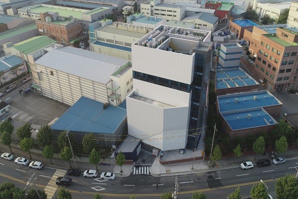
Merck announced on June 30th the grand opening of its advanced technology center (K-ATeC) in Songtan industrial complex.
Merck invested $29.2 million (35 billion KRW) in K-ATeC that will support R&D for chemical mechanical polishing (CMP) slurries and post-CMP cleaning. CMP slurry is used to smooth and planarize the surface of a semiconductor wafer.
K-ATeC is five stories tall and spans 3,240 m2. It is made up of a sampling lab for customer evaluation, a research lab that designs and analyzes CMP materials, and a cleanroom equipped with advanced equipment such as 300mm CMP wafer polishing system and wafer defect inspection equipment.
 <Merck opened K-ATeC that will focus on next semiconductor materials in Songtan industrial complex. The white building at the front is K-ATeC. (Reference: Merck) > <Merck opened K-ATeC that will focus on next semiconductor materials in Songtan industrial complex. The white building at the front is K-ATeC. (Reference: Merck) >It is unprecedented that Merck opened a R&D center for semiconductor materials in South Korea. Merck boasts a history of 352 years and it is a multinational chemical company that makes more than €16.2 billion (22 trillion KRW) in 2019 annual sales.
Merck recently acquired Versum Materials and Intermolecular one after the other, and these acquisitions are part of Merck’s plan to develop its semiconductor materials business. K-ATeC is an extension of Merck’s plan.
This investment shows that South Korea’s status within the global semiconductor industry is changing. Prior to the opening of K-ATeC, LAM Research decided to construct a R&D center in Gyeonggi-do. Another multinational semiconductor equipment maker TEL based in Japan finished constructing a mega customer support center in Pyeongtaek earlier this year.
Investments made by these multinational companies have been gaining speed since the Japanese Government imposed trade restrictions on South Korea last year. A multinational chemical company DuPont based in the U.S. also decided to construct an EUV (Extreme Ultraviolet) photoresist plant in Cheonan.
South Korea’s semiconductor industry was put into danger when the Japanese Government suddenly imposed trade restrictions. However, these restrictions have actually led to restructuring of the industry’s supply network centered on Samsung Electronics and SK Hynix and strengthened the industry’s ecosystem. As a result, multinational semiconductor companies that share same interests as the industry have started to enter the South Korean market one after the other and they have pushed South Korea as the key place for the global semiconductor industry.
“South Korea is an important hub not just for Merck, but for the entire semiconductor industry.” said Kai Beckmann who is the CEO for the Performance Materials business sector through an exclusive interview with the Electronic Times. “We are going to continue to put in efforts to make our supply network more flexible and we are also looking into focusing on the thin film and patterning fields through K-ATeC.”
Staff Reporter Yun, Geonil | benyun@etnews.com
<Source: Etnews> |